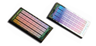
As the largest global supplier of bare die with access to thousands of different part types, we offers unparalleled knowledge & extensive capabilities as well as the flexibility to adapt our suppliers’ standard products to the unique requirements of your device or system. Over the years, we had developed and maintained key relationships with many of the leading semiconductor manufacturers providing us with the capability to offer an extensive bare die portfolio to our customers.
| Manufacturer |
DRAM |
Synch SRAM |
Asynch SRAM |
NAND Flash |
NOR Flash |
EEPROM |
MRAM |
FRAM&nvSRAM |
Download |
| Atmel |
|
|
|
|
|
✔ |
|
|
NULL |
| Cypress |
|
✔ |
✔ |
✔ |
✔ |
|
|
✔ |
NULL |
| Everspin |
|
|
|
|
|
|
✔ |
|
NULL |
| Microchip |
|
|
|
|
✔ |
✔ |
|
|
NULL |
| Micron |
✔ |
|
|
✔ |
✔ |
|
|
|
NULL |
| Northrop Grumman |
|
|
|
|
|
✔ |
|
|
NULL |
| Samsung |
✔ |
|
|
✔ |
|
|
|
|
NULL |
| ISSI |
✔ |
✔ |
✔ |
✔ |
✔ |
|
|
|
NULL |
| Alliance |
✔ |
✔ |
✔ |
|
|
|
|
|
NULL |
